


Generic
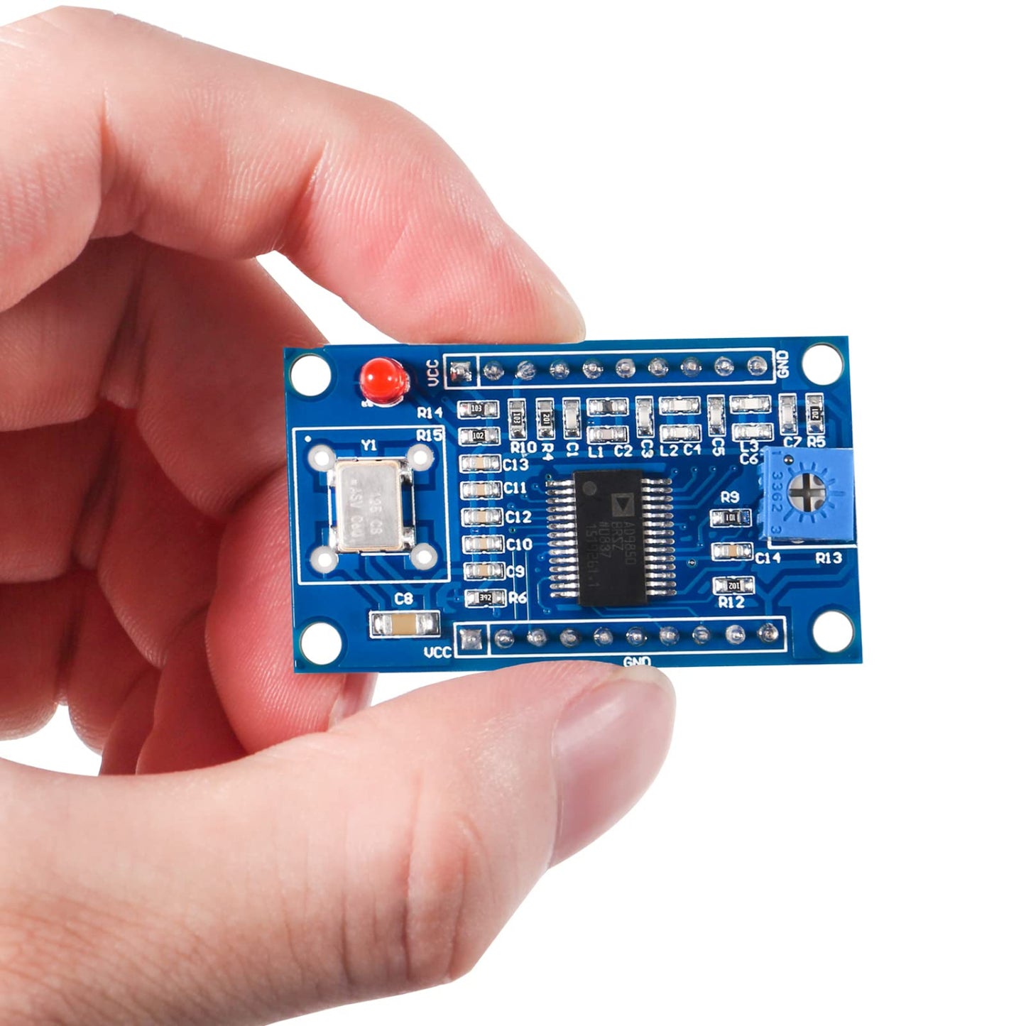
AD9850 DDS Signal Generator Module DDS Function Generator Module AD9850 Direct Digital Synthesizer Module For Electronics Projects- RS3566
AD9850 DDS Signal Generator Module DDS Function Generator Module AD9850 Direct Digital Synthesizer Module For Electronics Projects- RS3566
SKU:RS3566
Low stock: 6 left
Couldn't load pickup availability
- For Bulk Order Click Here
- Need Customer Support?
- Free Delivery Above 999/-
Note: In case you receive a damaged or faulty product, please return it in the original box with all foam and packaging. Returns will not be accepted if further damage occurs due to improper packing.
If you order a product that is currently in Preorder, and the price of that item increases in the future, you will be required to pay the difference in price.
For refund/return/replacement, call us at +91 95995 94520 or email us at support@rees52.com
Delivery Time
Delivery Time
- Delivery time with the Express Shipping option is 2-3 working days, and with the Standard Shipping option is 5-6 working days. It varies based on location, reliant on courier services.
- Delivery time if the order item is on Preorder Status is 15-20 working days.
COD (Cash on Delivery)
COD (Cash on Delivery)
- For COD you have to pay extra charges of Rs 350/- before the shipment. (We will share the company QR Code, UPI ID or Account details for the same)
Description:
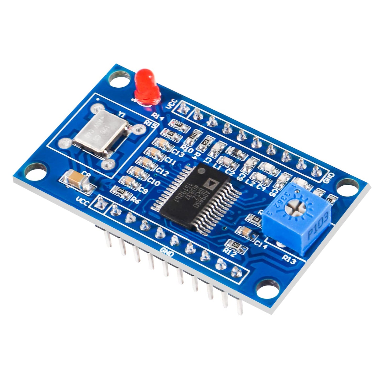
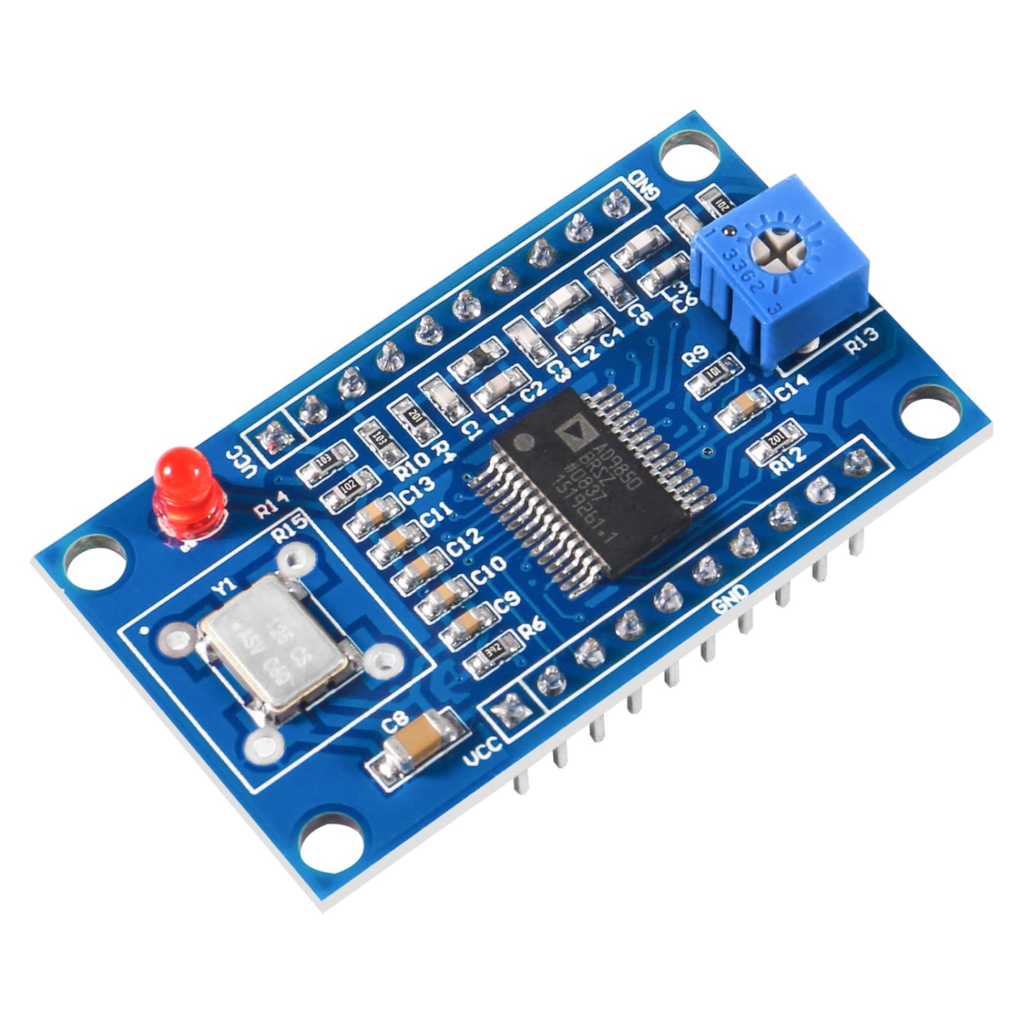
The AD9850 is a highly integrated device that uses advanced DDS technology coupled with an internal high speed, high performance, D/A converter and comparator, to form a complete digitally programmable frequency synthesizer and clock generator function.
DDS Function Generator Module all the external components which are needed are integrated on the board and the designer don’t need to care more about the detailed design of ADS9850. The designer only needs to add the power and control signals to driver this module
Specification:
- Operating Voltage: 3.3 – 6 Volts
- Oscillator Frequency: 125 MHz
- Output Frequency: 0 – 40 MHz
- Operational Temperature: -40 – 850C
- Source/Sink Continuous Current: 0.005 Amperes
- DAC Current: 0.03 Amperes
- Power Dissipation(125 MHz, 5V): 380 mWatts
- Power Dissipation(110 MHz, 3.3V): 110 mWatts
Features:
- DAC with Spurious Free Dynamic Range to specify the generator’s performance
- It contains a power-down function for a short boot time.
- Data transmission can either be parallel or serial.
- Power Dissipation depends on the power supply voltage.
- Four Analog signal outputs i.e., Sine-Wave 1, Sine-Wave 2, Square-Wave 1, and Square-Wave 2
- A comparator to generate less jittering in square wave output
- Direct Digital Synthesizer is based on CMOS Technology for better functionality and performance.
- A small high-performance module with a surface-mount package to be operated at industrial temperature
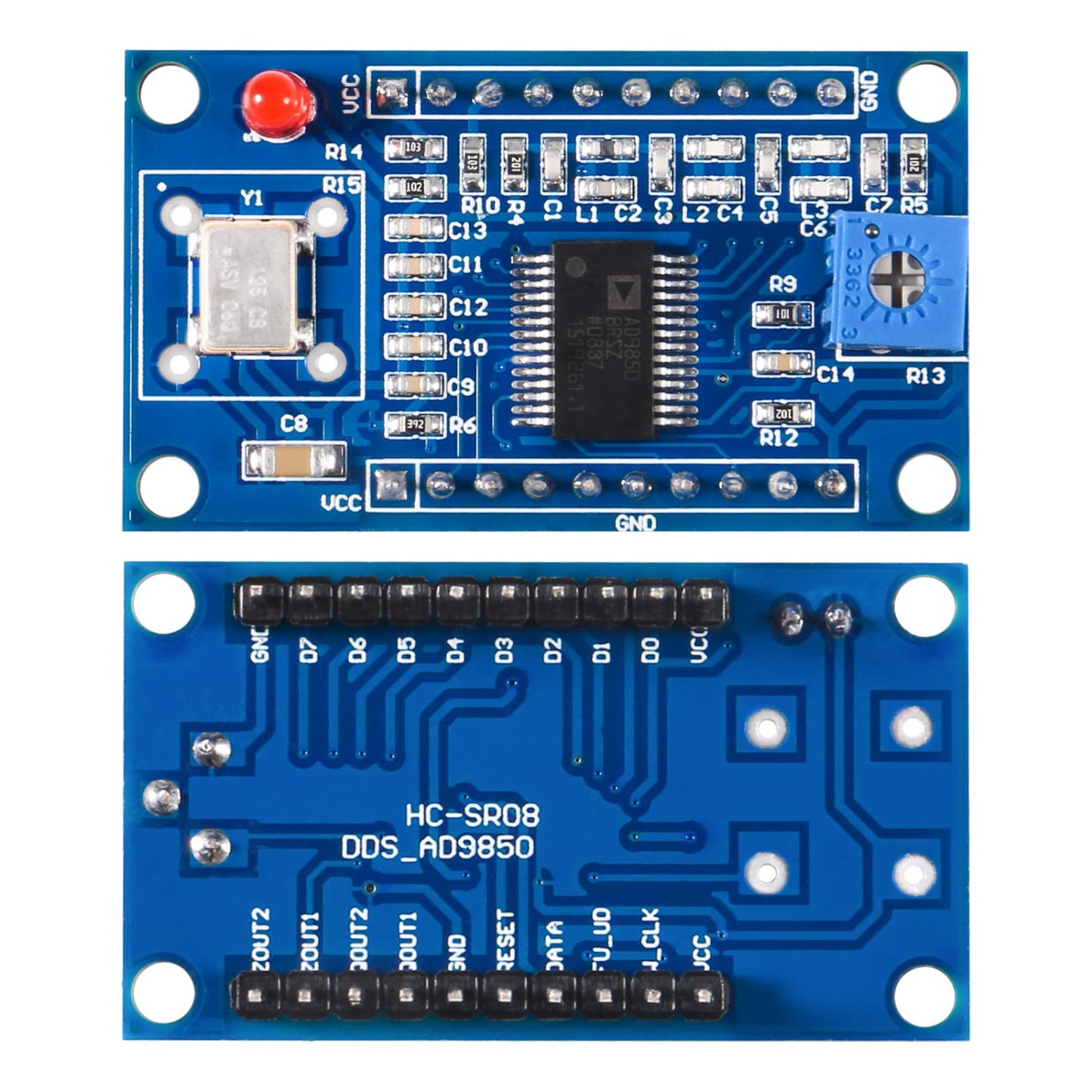
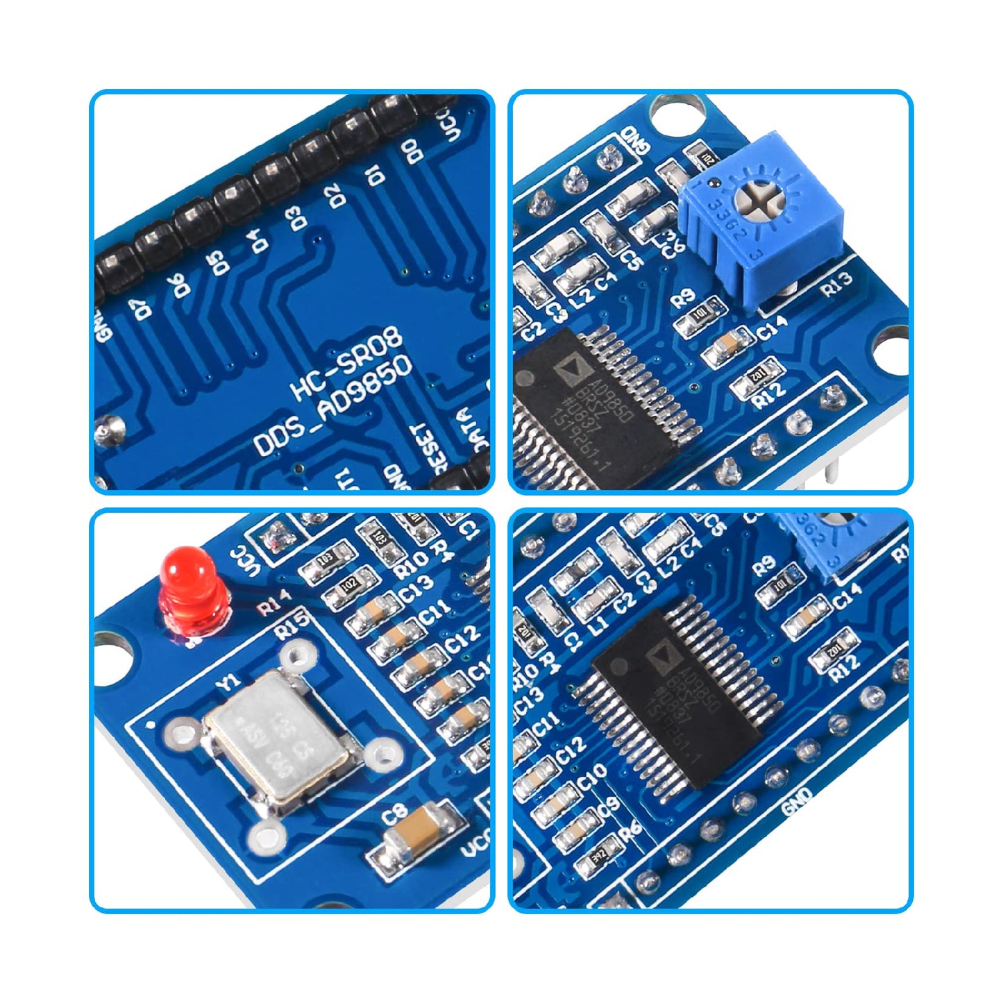
Pin Description:

- VCC: Supply pin
- D0-D7: Data input pin
- GND: Reference potential pin
- W-CLK: Word Load Clock pin
- FQ-UD: Frequency Update pin
- Data: Serial data input through D7 pin
- Reset: Master reset pin
- Sine-Wave 1: DAC Current Output pin
- Sine-Wave 2: DAC Current Output pin
- Square-Wave 1: DAC Complementary Output pin
- Square-Wave 2: DAC Complementary Output pin
- Input/Output pins: These are 8-bit data pins used to load data up to 32-bit frequency and 8-bit phase/control word. D7(MSB) also serves the purpose of loading a 40-bit serial data word.
- W-CLK: A Word Load Clock is used to synchronize and load words serially or through parallel transmission.
- FQ-UD: Frequency Update is used to update the frequency in the input data register when the clock has a rising edge. After updating, it reset the pointer to the word 0
- DATA: This pin is connected to the D7 input pin. It is used to load serial data.
- RESET: A master RESET is used to clear all the registers except for the IC’s input register by putting it into a HIGH state. Moreover, the outputs of DAC will be converted to Cosine 0 after some clocks.
Useful Link:
Package Included:
1 x AD9850 DDS Signal Generator Module DDS Function Generator Module AD9850 Direct Digital Synthesizer Module For Electronics Projects