- Type - p-n-p
- Collector-Emitter Voltage: -25 V
- Collector-Base Voltage: -40 V
- Emitter-Base Voltage: -5 V
- Collector Current: -0.5 A
- Collector Dissipation - 0.625 W
- DC Current Gain (hfe) - 85 to 300
- Transition Frequency - 150 MHz
- Operating and Storage Junction Temperature Range -65 to +150 °C
Description
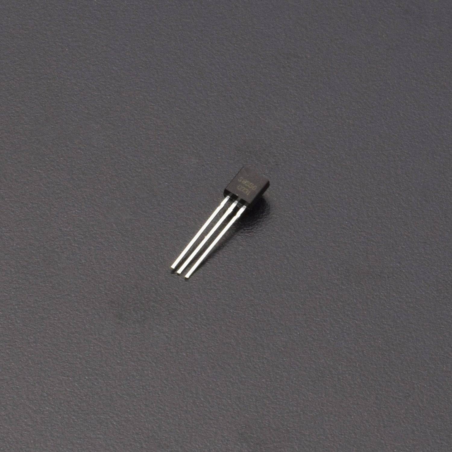
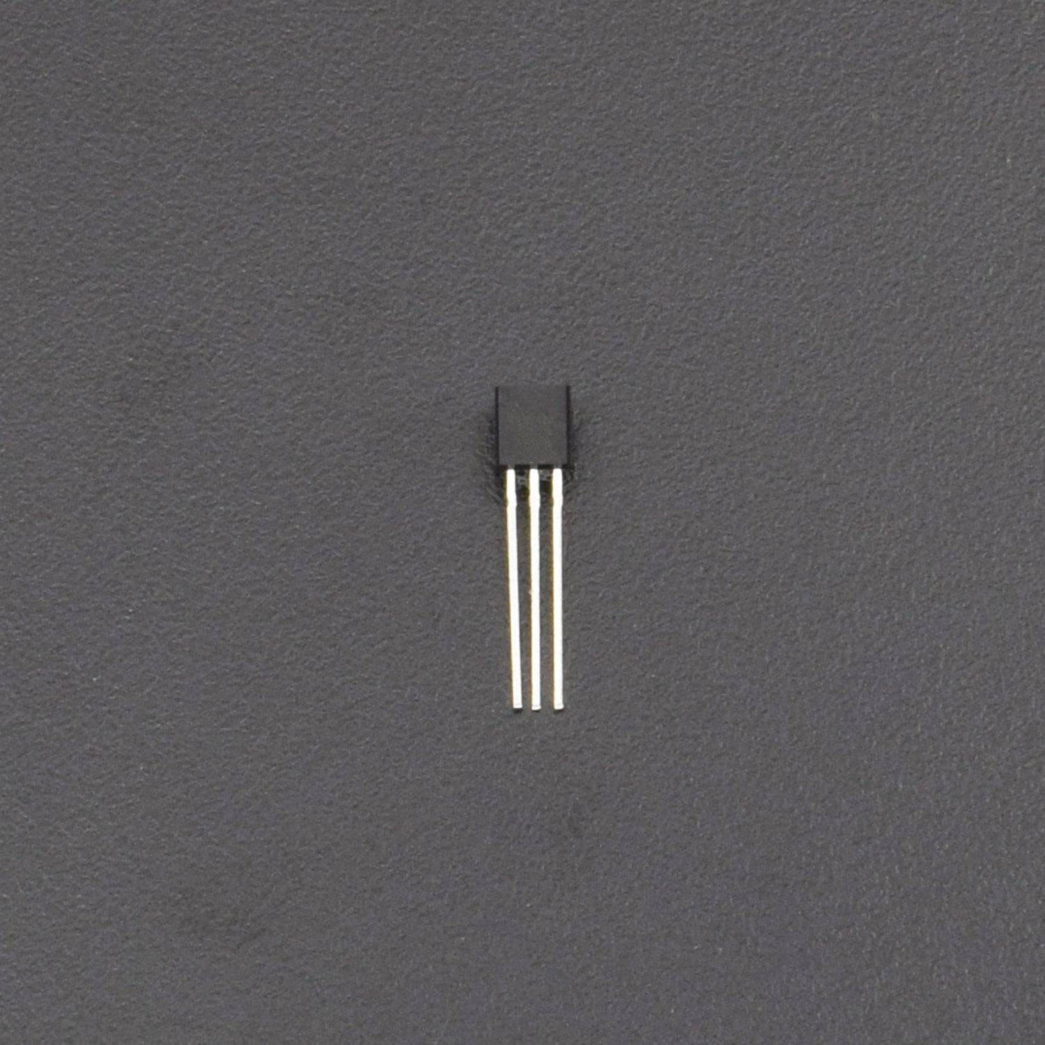
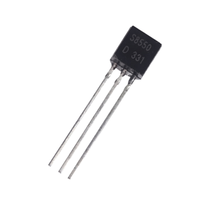
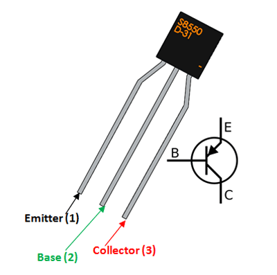
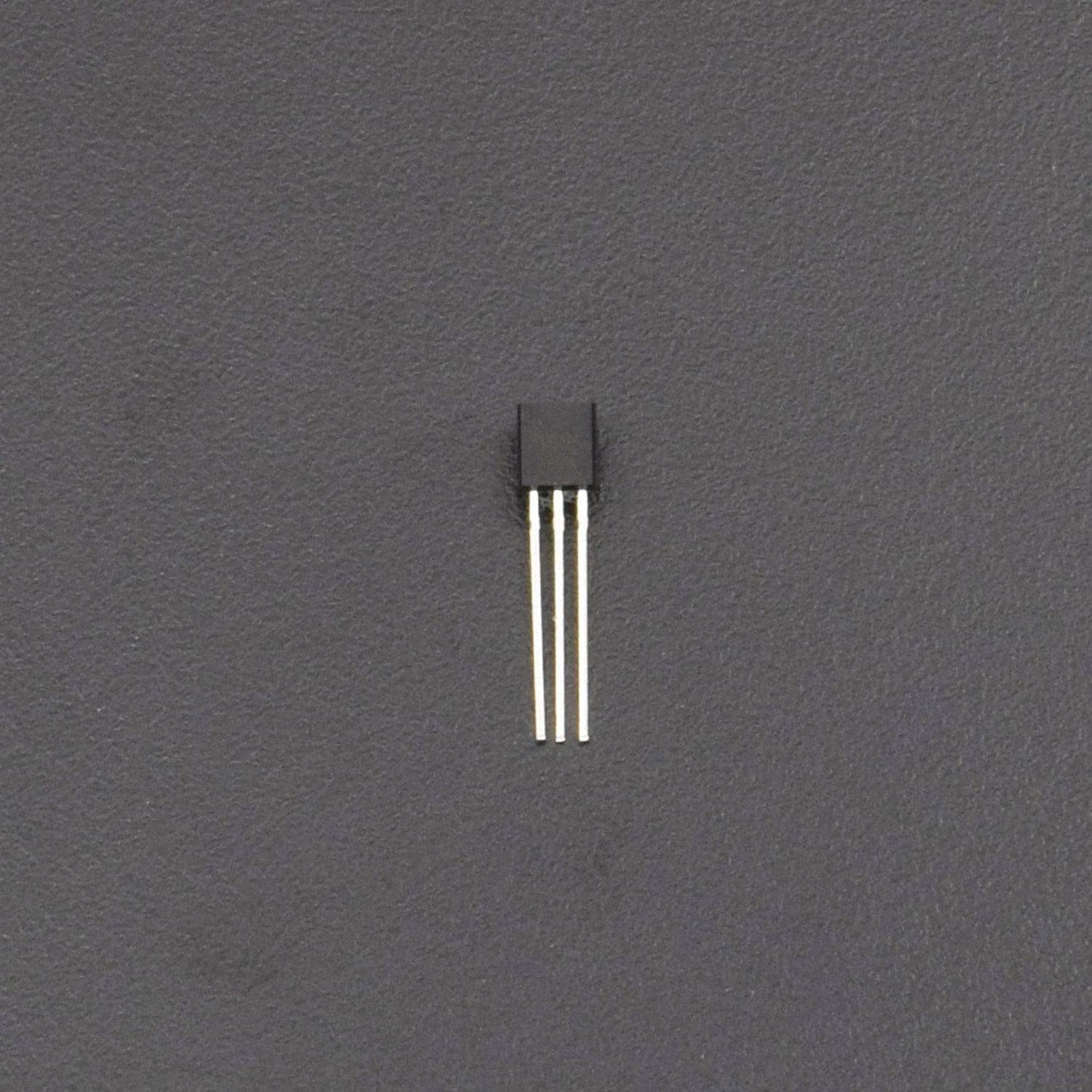
The S8550 is manufactured in a plastic TO-92 case. When looking at the flat side with the leads pointed downward, the three leads emerging from the transistor are, from left to right, the emitter, base, and collector leads.
S8550 Pinout Configuration
Pin Number |
Pin Name |
Description |
1 |
Emitter |
Current Drains out through emitter, normally connected to ground |
2 |
Base |
Controls the biasing of the transistor, Used to turn ON or OFF the transistor |
3 |
Collector |
Current flows in through collector, normally connected to load |
Features
- Type - p-n-p
- Collector-Emitter Voltage: -25 V
- Collector-Base Voltage: -40 V
- Emitter-Base Voltage: -5 V
- Collector Current: -0.5 A
- Collector Dissipation - 0.625 W
- DC Current Gain (hfe) - 85 to 300
- Transition Frequency - 150 MHz
- Operating and Storage Junction Temperature Range -65 to +150 °C


